Dont forget dimensioning of allowed gate cap in accordance with driving capability of said drivers ![]()
Funny how symmetry plays such a great role in electronics. From silicon chips and even PCB design ![]()
Dont forget dimensioning of allowed gate cap in accordance with driving capability of said drivers ![]()
Funny how symmetry plays such a great role in electronics. From silicon chips and even PCB design ![]()
Why add parts to the design if the parts cost more than replacing blown units?
Yes, particularly if you don’t replace them anyway, or charge a ridiculous price for replacement insurance.
IT’S A FOCKING BEAST!!!
And it’s very much alive. Tests are great so far - Low noise levels, and overall very convincing.
BUT, there are a few pads I need to move further apart to avoid erroneous boards from jlcpcb. And then a few cosmetic things.
Now, I need to test that the IMU, CAN, SRV-port (for remote control), NRF-24 addon works, etc.
Release-party coming up.
The board upon arrival from jlcpcb. Sorry, you will need a saw… Needs to be like this to avoid getting extra charged by the pcb manufacturer. I will try to minimize the paths to be sawed in coming orders, to see how far I can push it. Don’t know if I can make a deal with them, because it is only one board (in modules).
Att., 12 holes for solid mounting of each mosfet to aluminum back plate.
Excellent! Glad to see this moving forward.
I know that everyone quotes the room temp junction pulse current rating, it’s such a wonderfully high number. But that 207A rating for your FETs is a theoretical number for a microseconds long pulse (at most) that leaves the junction at room temp. It can’t be used for anything practical.
Sweet! Dumb question though… Did you do a “solder-only” attachment of the processor board to avoid noise, prevent it coming loose, or just for the heck of it? How safe do you think it would be to mount it on pin headers and sockets - if also mechanically secured?
Also, I’m assuming JLCPCB did all the surface mount stuff, including the processor, right?
Me neither! But you seem to know what you’re doing ![]()
I know the board is not going to run at 2x207A = 414 Amps! That’s an insane number. At 75V the losses to heat would be enough to heat a house at winter time, and obviously everything would desolder.
Electromagnetic induced noise and oscillations are what eventually will kill the board as power turns in eastern directions. A short circuit when a mosfet is self triggered at some point.
Good comments here! Thank you for pointing out that I do in fact not have a seperate gate resistor for each FET. This is a mistake from my side, and I do need to fix that. SDFJAHKT!!
Luckily, I only need to reorder the “main board” part, so I guess it will be 1/3 of the price.
This picture shows the design of a single phase in the schematics of the MP2 design. Mr. Battery_Mooch, I would like to hear your comments on this… ?
I don’t know what I’m doing, but I know that I’m doing something… (btw, Is this quote already taken?)
HUGE MISTAKE !!!
We’re starting to get into consulting territory here. ![]() But I’m happy to give some quick thoughts…
But I’m happy to give some quick thoughts…
IMO this will lead to disaster most of the time.
You can take out most of the inter-connecting board material using a line of spaced out slots and then adding “mouse bites” using unplated holes in the remaining material segments in order to make snapping the boards apart much easier.
You only need to leave enough material to hold the boards together during manufacture/assembly. Make sure any copper planes are kept out of this space between boards.
Take into account the forces used to snap the boards apart and how that might bend the boards and stress the component solder joints. Consider where fingers might be placed when doing this. You might need to have a graphic showing where to place fingers and how to safely snap them apart without stressing the board.
Sorry for doing the drawing in MoochCAD…
I would think a Dremel cut-off wheel would safely separate them - no?
It could work but not safely IMO…one slip could damage the board or a component. It also creates huge amounts of static which can easily fry components. Not everyone has a Dremel too. ![]()
I looked on youtube for that old SNL fake commercial where they perform a circumcision in the back of a Lincoln Town Car, but couldn’t find it. ![]()
I really appreciate your help here… Thanks!
But, this one I tried already, and were to be charged an extra 50 dollars for adding mouse bites.
A dremel cut off wheel is impossible to control, use a small manual saw like this:
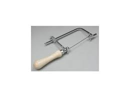
Use small manual saw


